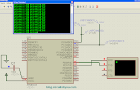
In this Analog to Digital Conversion tutorial we get answers to following questions.
1. How to Configure internal ADC of AVR Microcontroller?
2. How to select ADC Channel?
3. How to set sampling rate?
4. How to make Voltmeter using ADC?
To operate AVR internal ADC you need three registers these are
1. ADMUX- Channel and Reference Voltage selection
2. ADCSRA- ADC Control and Status Register
3. ADC (ADCH:ADCL) - ADC Conversion result
Overview :
The ATmega8A features a 10-bit successive approximation ADC. The ADC is connected to an 8-channel Analog Multiplexer which allows eight single-ended voltage inputs constructed from the pins of Port C. The single-ended voltage inputs refer to 0V (GND). The ADC contains a Sample and Hold circuit which ensures that the input voltage to the ADC is held at a constant level during conversion. The ADC has a separate analog supply voltage pin, AVCC. AVCC must not differ more than ± 0.3V from VCC. Internal reference voltages of nominally 2.56V or AVCC are provided On-chip. The voltage reference may be externally decoupled at the AREF pin by a capacitor for better noise performance. The ADC converts an analog input voltage to a 10-bit digital value through successive approximation. The minimum value represents GND and the maximum value represents the voltage on the AREF pin minus 1 LSB. Optionally, AVCC or an internal 2.56V reference voltage may be connected to the AREF pin by writing to the REFSn bits in the ADMUX Register. The internal voltage reference may thus be decoupled by an external capacitor at the AREF pin to improve noise immunity.
The analog input channel is selected by writing to the MUX bits in ADMUX. Any of the ADC input pins, as well as GND and a fixed bandgap voltage reference, can be selected as single ended inputs to the ADC. The ADC is enabled by setting the ADC Enable bit, ADEN in ADCSRA. Voltage reference and input channel selections will not go into effect until ADEN is set. The ADC does not consume power when ADEN is cleared, so it is recommended to switch off the ADC before entering power saving sleep modes. The ADC generates a 10-bit result which is presented in the ADC Data Registers, ADCH and ADCL. By default, the result is presented right adjusted, but can optionally be presented left adjusted by setting the ADLAR bit in ADMUX. If the result is left adjusted and no more than 8-bit precision is required, it is sufficient to read
ADCH. Otherwise, ADCL must be read first, then ADCH, to ensure that the content of the Data Registers belongs to the same conversion. Once ADCL is read, ADC access to Data Registers is blocked. This means that if ADCL has been read, and a conversion completes before ADCH is read, neither register is updated and the result from the conversion is lost. When ADCH is read, ADC access to the ADCH and ADCL Registers is re-enabled. The ADC has its own interrupt which can be triggered when a conversion completes. When ADC access to the Data Registers is prohibited between reading of ADCH and ADCL, the interrupt will trigger even if the result is lost.
Starting a Conversion:
A single conversion is started by writing a logical one to the ADC Start Conversion bit, ADSC. This bit stays high as long as the conversion is in progress and will be cleared by hardware when the conversion is completed. If a different data channel is selected while a conversion is in progress, the ADC will finish the current conversion before performing the channel change.
ADC Voltage Reference:
The reference voltage for the ADC (VREF) indicates the conversion range for the ADC. Single ended channels that exceed VREF will result in codes close to 0x3FF. VREF can be selected as either AVCC, internal 2.56V reference, or external AREF pin.
ADC Conversion Result:
After the conversion is complete (ADIF is high), the conversion result can be found in the ADC Result Registers (ADCL, ADCH). For single ended conversion, the result is
Important Registers Required to Configure ADC:
ADMUX: ADC Multiplexer Selection Register
This register is used to select Reference Voltage and Analog Input Channel
• Bit 7:6 – REFS1:0: Reference Selection Bits
These bits select the voltage reference for the ADC, as shown in Table. If these bits are changed during a conversion, the change will not go in effect until this conversion is complete (ADIF in ADCSRA is set). The internal voltage reference options may not be used if an external reference voltage is being applied to the AREF pin.
• Bit 5 – ADLAR: ADC Left Adjust Result
The ADLAR bit affects the presentation of the ADC conversion result in the ADC Data Register. Write one to ADLAR to left adjust the result. Otherwise, the result is right adjusted. Changing the ADLAR bit will affect the ADC Data Register immediately, regardless of any ongoing conversions.
ADCL and ADCH – The ADC Data Register
ADLR=0
ADLR=1
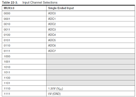
• Bits 3:0 – MUX3:0: Analog Channel Selection Bits
The value of these bits selects which analog inputs are connected to the ADC. See Table 22-3
for details. If these bits are changed during a conversion, the change will not go in effect until this
conversion is complete (ADIF in ADCSRA is set).
ADCSRA – ADC Control and Status Register A
• Bit 7 – ADEN: ADC Enable
Writing this bit to one enables the ADC. By writing it to zero, the ADC is turned off. Turning the ADC off while a conversion is in progress, will terminate this conversion.
• Bit 6 – ADSC: ADC Start Conversion
In Single Conversion mode, write this bit to one to start each conversion. In Free Running mode, write this bit to one to start the first conversion. The first conversion after ADSC has been written after the ADC has been enabled, or if ADSC is written at the same time as the ADC is enabled, will take 25 ADC clock cycles instead of the normal 13. This first conversion performs initialization of the ADC. ADSC will read as one as long as a conversion is in progress. When the conversion is complete, it returns to zero. Writing zero to this bit has no effect.
• Bit 5 – ADFR: ADC Free Running Select
When this bit is set (one) the ADC operates in Free Running mode. In this mode, the ADC samples and updates the Data Registers continuously. Clearing this bit (zero) will terminate Free Running mode.
• Bit 4 – ADIF: ADC Interrupt Flag
This bit is set when an ADC conversion completes and the Data Registers are updated. The ADC Conversion Complete Interrupt is executed if the ADIE bit and the I-bit in SREG are set. ADIF is cleared by hardware when executing the corresponding interrupt Handling Vector. Alternatively, ADIF is cleared by writing a logical one to the flag. Beware that if doing a Read-Modify- Write on ADCSRA, a pending interrupt can be disabled. This also applies if the SBI and CBI instructions are used.
• Bit 3 – ADIE: ADC Interrupt Enable
When this bit is written to one and the I-bit in SREG is set, the ADC Conversion Complete Interrupt is activated.
• Bits 2:0 – ADPS2:0: ADC Prescaler Select Bits
These bits determine the division factor between the XTAL frequency and the input clock to the ADC.
This is what we need:
  ADMUX=0xC0;    //Select Channel 0 and Internal Ref 2.56V
  ADCSRA=0xC7;   //ADEN=1, ADSC=1 Start Conversion, ADFR=0,ADIF=0,                                //Prescalar=128 Slow for Voltage Measurement
  while (!(ADCSRA & (1<<ADIF))); //Wait until Conversion Completes
  value=ADC;
  ADCSRA |= 1<<4; //Clear ADIF Flag
Practical Design will give you clear Idea of internal ADC of AVR Microcontroller:
Lets make a voltmeter that will measure the voltage and send data serially to PC.
AVR Studio Code:
#include <avr/io.h>

#define FOSC 8000000// 8Mhz Clock Speed
#define BAUD 9600
#define MYUBRR FOSC/16/BAUD-1

void USART_Transmit( unsigned char data );
void USART_Init( unsigned int ubrr);
unsigned char USART_Receive( void );
void SendString(char mydata[20]);
/*******************************************************/
void main( void )
{
   char mychar[5];       //variable to hold ASCII values
   int value;
   USART_Init (MYUBRR);

   while(1)
   {

  ADMUX=0xC0;    //Select Channel 0 and Internal Ref 2.56V
  ADCSRA=0xC7;   //ADEN=1, ADSC=1 Start Conversion, ADFR=0,ADIF=0, Prescalar=128 Slow for Voltage Measurement
  while (!(ADCSRA & (1<<ADIF))); //Wait until Conversion Completes
  value=2.5*ADC;
  ADCSRA |= 1<<4; //Clear ADIF Flag

        //10-bit=1024 value for 2.56V
  //Vin=(2.56/1024)*ADC
  //We know that flowting point operation slow down the microcontroller
  //So we take it as  Vin=(2560/1024)*ADC
  //as we have multiplied it by 1000 so what ever comes we put fixed decimal point 0.000

        SendString("Voltage1:");
     sprintf(mychar,"%04d",value);  //This will convert integer into ASCII array
        USART_Transmit(mychar[0]);  //First Digit
        USART_Transmit('.');        //Decimal Point
     USART_Transmit(mychar[1]);  //Second Digit
  USART_Transmit(mychar[2]);
        USART_Transmit(mychar[3]);

//Similarly display for second channel

  ADMUX=0xC1;    //Select Channel 1 and Internal Ref 2.56V
  ADCSRA=0xC7;   //ADEN=1, ADSC=1 Start Conversion, ADFR=0,ADIF=0, Prescalar=128 Slow for Voltage Measurement
  while (!(ADCSRA & (1<<ADIF))); //Wait until Conversion Completes
  value=2.5*ADC;
  ADCSRA |= 1<<4; //Clear ADIF Flag


        SendString(" Voltage2:");
     sprintf(mychar,"%04d",value);  //This will convert integer into ASCII array
        USART_Transmit(mychar[0]);  //First Digit
        USART_Transmit('.');        //Decimal Point
     USART_Transmit(mychar[1]);  //Second Digit
  USART_Transmit(mychar[2]);
        USART_Transmit(mychar[3]);
        USART_Transmit(13); //Line break
   }
}

/*******************************************************/
void USART_Init( unsigned int ubrr)
{
    /* Set baud rate */
     UBRRH = (unsigned char)(ubrr>>8);
     UBRRL = (unsigned char)ubrr;
    /* Enable receiver and transmitter */
     UCSRB = (1<<RXEN)|(1<<TXEN);
    /* Set frame format: 8data, 2stop bit */
     UCSRC = (1<<URSEL)|(1<<USBS)|(3<<UCSZ0);
}

/*******************************************************/
void USART_Transmit( unsigned char data )
{
   /* Wait for empty transmit buffer */
   while ( !( UCSRA & (1<<UDRE)) );
  /* Put data into buffer, sends the data */
   UDR = data;
}
/*******************************************************/
unsigned char USART_Receive( void )
{
   /* Wait for data to be received */
    while ( !(UCSRA & (1<<RXC)) );
   /* Get and return received data from buffer */
   return UDR;
}
/*******************************************************/
void SendString(char mydata[20])
{
  int i;
   for(i=0;i<strlen(mydata);i++)
   {
     USART_Transmit(mydata[i]);
   }
}
/*******************************************************/


No comments:
Post a Comment